
This is a Wishbone to SPI bridge that converts Wishbone transactions from a host into SPI-memory transactions. It can be used to map a SPI flash, EEPROM or RAM into the address space of a processor. The bridge operates transparently, so it behaves like a memory-mapped read/write memory as it hides the SPI protocol - at the cost of additional latency. Hence, the bridge supports Execute-In-Place (XIP) allowing a processor to directly access (and execute) instructions and data located in the SPI memory.
ℹ️ This is another "spin-off" project of the NEORV32 RISC-V Processor. The bridge might be added as XIP module to the processor someday.
Key features
- Wishbone b4 compatible, classic or pipelined single-access transfers
- supports execute-in-place (XIP)
- single clock domain
- configurable SPI clock speed, clock mode (0,1,2,3) and address size
- supports 32-bit, 16-bit and 8-bit write accesses
- little-endian byte-order
- technology, vendor and platform agnostic
- single VHDL file, no additional libraries required
- FPGA-proven
TODOs / Ideas / Help-Wanted
- add burst support
- add dSPI/qSPI support
- check SPI flash status register during write
- ...
The bridge is based on a single VHDL file rtl/wb_spi_bridge.vhd.
The top entity is wb_spi_bridge, which can be instantiated directly without the need for any special libraries.
entity wb_spi_bridge is
  generic (
    SPI_CLK_DIV  : positive;   -- clock divider: f(spi_clk_o) = f(clk_i) / 2*SPI_CLK_DIV, min 2
    SPI_ABYTES   : positive;   -- number of address bytes in SPI protocol, 1..4
    SPI_CPHA     : std_ulogic; -- clock phase
    SPI_CPOL     : std_ulogic; -- idle polarity
    WB_ADDR_BASE : std_ulogic_vector(31 downto 0); -- module base address, size-aligned
    WB_ADDR_SIZE : positive    -- module address space in bytes
  );
  port (
    -- wishbone host interface --
    wb_clk_i   : in  std_ulogic; -- clock
    wb_rstn_i  : in  std_ulogic; -- reset, async, low-active
    wb_srstn_i : in  std_ulogic; -- reset, SYNC, low-active
    wb_adr_i   : in  std_ulogic_vector(31 downto 0); -- address
    wb_dat_i   : in  std_ulogic_vector(31 downto 0); -- read data
    wb_dat_o   : out std_ulogic_vector(31 downto 0); -- write data
    wb_we_i    : in  std_ulogic; -- read/write
    wb_sel_i   : in  std_ulogic_vector(03 downto 0); -- byte enable
    wb_stb_i   : in  std_ulogic; -- strobe
    wb_cyc_i   : in  std_ulogic; -- valid cycle
    wb_ack_o   : out std_ulogic; -- transfer acknowledge
    wb_err_o   : out std_ulogic; -- transfer error
    -- SPI device interface --
    spi_csn_o  : out std_ulogic; -- chip-select, low-active
    spi_clk_o  : out std_ulogic; -- serial clock
    spi_data_i : in  std_ulogic; -- device data output
    spi_data_o : out std_ulogic  -- controller data output
  );
end wb_spi_bridge;
The top entity instantiates two in-file entities:
wb_spi_bridge_linkhandles the SPI memory protocol (read, write, write-enable)wb_spi_bridge_phyhandles the actual serial peripheral interface protocol
wb_rstn_i) and a synchronous one (wb_srstn_i),
which are both are low-active. The asynchronous reset is required to bring the bridge into a defined state. The
synchronous reset is optional and can be used to reset the bridge from the application logic. Tie this reset to 1
if it is not used.
The application-specific configuration of the Wishbone-to-SPI bridge is done using the generics of the top entity.
The SPI clock frequency is configures using the SPI_CLK_DIV generic. It defines a scaler that is applies to the
clock input clk_i to obtain the actual SPI clock. The SPI clock is defined by f_spi = f_main / (2 * SPI_CLK_DIV).
The minimum allowed value for the clock scaler is 2 resulting in a maximal SPI clock speed of 1/4 of the input clock speed.
The actual clock mode is configured via SPI_CPHA and SPI_CPOL. The combination of these two generics allow to
configure any of the four standard SPI clock modes. For more information regarding the clock modes see the
SPI Wikipedia article.
The address size of the SPI memory, which is defined by it's capacity, is configured by the SPI_ABYTES generic.
Allowed values are 1, 2, 3 and 4. Most SPI EEPROMs use an address size of 16-bit resulting in SPI_ABYTES = 2. Many
standard SPI flash memories use 24-bit for the addressing resulting in SPI_ABYTES = 3.
The bridge uses only three standard memory commands. If the commands of a specific SPI memory are different, you can adapt them in the VHDL source file:
-- spi memory opcodes -----------------------------------------------------------
constant cmd_write_c : std_ulogic_vector(7 downto 0) := x"02"; -- write data
constant cmd_read_c  : std_ulogic_vector(7 downto 0) := x"03"; -- read data
constant cmd_wren_c  : std_ulogic_vector(7 downto 0) := x"06"; -- write enable
-- ------------------------------------------------------------------------------The 32-bit base address of the bridge is defined by the WB_ADDR_BASE generic. The size of occupied address space, which
is defined the SPI memory's capacity, is configured by the WB_ADDR_SIZE generic. The address space size has to be
a power of two and the base address has to be naturally aligned to the this size.
Example: SPI flash with 64kB (64*1024 bytes):
WB_ADDR_BASE => 0x"FFFF0000",
WB_ADDR_SIZE => 64*1024
❌ In this case a base address of 0xFFFF8000 would be invalid as it is not naturally aligned to a 64kB boundary.
The host interface is based on the Wishbone b4 specification. It supports classic and pipelined single-access transfers. Burst transfer are not supported yet.
| Classic-mode read access example | Pipelined-mode write access example |
|---|---|
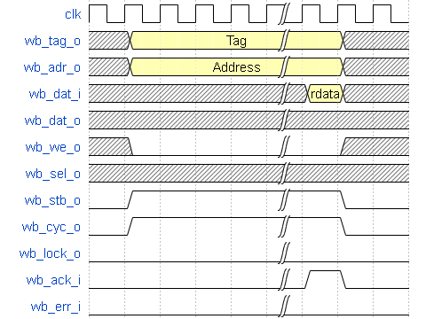 |
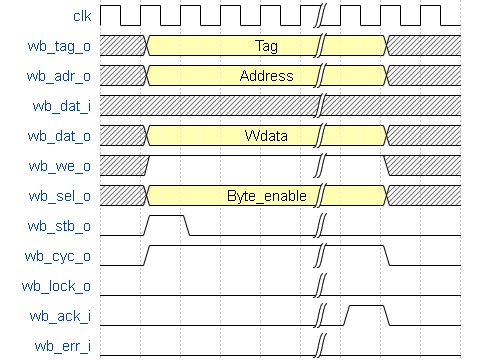 |
- classic-mode:
stbandcycboth stay asserted until the transfer is completed. - pipelined-mode:
cycstays asserted until the transfer is completed.stbis asserted only for one cycle right at the beginning of the transfer. |
A transfer is completed when the acknowledge signal ack is set (active for one cycle). This indicates a successful
termination. A transfer is also completed when the error signal err is set (active for one cycle) indicating
an erroneous termination. The bridge will raise the error signal only if an unsupported byte-enable mask is set
(see below).
The bridge supports 32-bit, 16-bit and 8-bit write accesses. Read accesses always return a full 32-bit word.
Note that the bridge accesses memory data in little-endian byte-order.
The sel byte mask signal defines the data quantity of the according access. The following byte masks are supported:
sel |
r/w | Data quantity |
|---|---|---|
1111 |
read | full 32-bit word |
1111 |
write | full 32-bit word |
1100 |
write | upper 16-bit half-word |
0011 |
write | lower 16-bit half-word |
0001 |
write | byte 0 |
0010 |
write | byte 1 |
0100 |
write | byte 2 |
1000 |
write | byte 3 |
All remaining byte mask combination will raise a transfer error (err is set for one cycle instead of ack).
The bridge always sends a complete command sequence to the SPI memory for any kind of Wishbone transfer (bursts are not supported yet). This means that the memory opcode, the address bits and the actual data are transferred for every single transaction. The following table shows the number of bit to transfer via SPI for each type of transaction. Each bit requires one clock of the SPI clock.
| r/w | Data size | CMD bits | Address bits | Data bits | Total bits |
|---|---|---|---|---|---|
| read | word (32-bit) | 8 |
8*SPI_ABYTES |
32 |
8 + 8*SPI_ABYTES + 32 |
| write | word (32-bit) | 8 + 8 |
8*SPI_ABYTES |
32 |
8 + 8 + 8*SPI_ABYTES + 32 |
| write | half-word (16-bit) | 8 + 8 |
8*SPI_ABYTES |
16 |
8 + 8 + 8*SPI_ABYTES + 16 |
| write | byte (8-bit) | 8 + 8 |
8*SPI_ABYTES |
8 |
8 + 8 + 8*SPI_ABYTES + 8 |
For example a word-wide write access to a SPI flash that uses 24-bit addressing requires
8 + 8 + 8*3 + 32 = 72 SPI clock cycles. One SPI clock cycle equals 2 * SPI_CLK_DIV cycles of the main
clock clk_i.
ℹ️ Any kind of write access requires to set the memory's write enable latch, which is done sending a single 8-bit command.
The projects provides a simple testbench sim/wb_spi_bridge_tb.vhd,
which can be simulated by GHDL via the provides script:
wb_spi_bridge/sim$ sh ghdl.shThe simulation will run for 1ms using a 100MHz clock. During this time all supported (and one illegal) Wishbone
accesses are triggered. Note that this testbench is intended for manual waveform inspection - it is not self-checking!
The waveform data is stored to sim/wb_spi_bridge.vcd, which can be viewed by using gtkwave:
wb_spi_bridge/sim$ gtkwave wb_spi_bridge.vcdThe bridge is FPGA-proven. It has been tested by directly connecting it to the Wishbone interface port of the NEORV32 RISC-V Processor (no Wishbone interconnect) interfacing a 25LC512 SPI EEPROM.
The NEORV32 software examples provides a "bus explorer" program that allows to perform arbitrary Wishbone accesses via a UART terminal. The bridge can successfully handle all read and write operations. Furthermore, the NEORV32 can successfully execute in place programs from the SPI module.
Exemplary mapping results for the following configuration :
SPI_CLK_DIV  => 32,
SPI_ABYTES   => 2, -- 16-bit addressing
SPI_CPHA     => '0',
SPI_CPOL     => '0', -- clock mode 0
WB_ADDR_BASE => x"F0000000",
WB_ADDR_SIZE => 64*1024Hierarchy Logic Cells Logic Registers
----------------------------------------------------------------------------
wb_spi_bridge:wb_spi_bridge_inst 233 (115) 174 (88)
wb_spi_bridge_link:wb_spi_bridge_link_inst 118 (16) 86 (8)
wb_spi_bridge_phy:wb_spi_bridge_phy_inst 102 (102) 78 (78)